| ��ǰλ�ã����->���g���� |
|
| INA1620�߱������l�\��Ŵ�����Q���� |
|
|
| ����Դ���������Ƽ� ���r�g��2020/1/17 11:11:00 |
�ھ���ԃ�� |
| |
TI��˾��INA1620�Ǽ����˾���ƥ��ı�Ĥ��茦��EMI�V�����ĸ߱������l�\��Ŵ���,���е�ʧ���ݔ������ɂ����l�\��Ŵ���.�Ŵ����ĵ������ܶȞ�2.8-nV/��Hz,1 kHz��THD+N��-119.2dB,150mWݔ�����ʕr����32-��ؓ�d.���ɵı�Ĥ���ƥ�����0.004%��,�����Á턓�������ķdz������ܵ����l�·.INA1620����늉���2 V �� ��18 V,ÿ·����H��2.6mA.�����P��ģʽʹ�Ŵ����Ĵ��C���С��5 ��A.�Ŵ������控����21MHz(G=+1000),�D�Q���ʞ�10 V/��s,���ؓ�d����������600 pF,600-��ؓ�d�r���_·�����136dB,�����Ĺ����ضȏĨC40�� ��+125��.��Ҫ���ڸ߱���(HiFi)���C����,���I���l�O��,ģ�M�͔��ֻ�Ͽ����_,���l�yԇ�͜y��.���Ľ�B��INA1620��Ҫ����,���ܿ�D�Ͷ��C�Ŵ��������·,���I�����L�A�Ŵ����·�Լ����l�Ŵ����u��ģ�KINA1620 EVM��Ҫ����,�·�D,������κ�PCB�OӋ�D.
The INA1620 integrates 4 precision-matched thin-filmresistor pairs and EMI filtering on-chip with a lowdistortion,high output current, dual audio operationalamplifier. The amplifier achieves a very low,2.8-nV/��Hz noise density with an ultra-low THD+N of�C119.2 dB at 1 kHz and drives a 32-�� load at 150-mW output power. The integrated thin-film resistorsare matched to within 0.004% and can be used tocreate a large number of very high-performanceaudio circuits.
The INA1620 operates over a very wide supply rangeof ��2 V to ��18 V on only 2.6 mA of supply current perchannel. The INA1620 also has a shutdown mode,allowing the amplifiers to be switched from normaloperation to a standby current that is typically less��than 5 ��A. Shutdown mode is specifically designed toeliminate click-and-pop noise when transitioning intoor out of shutdown mode.
The INA1620 has a unique internal layout for lowestcrosstalk, and freedom from interactions betweenchannels, even when overdriven or overloaded. Thisdevice is specified from �C40�� to +125��.
The INA1620 integrates a dual, bipolar-input, audio operational amplifier with four high-precision thin-film resistorpairs on the same die. The internal amplifiers and resistor pairs are pinned out to allow for many circuitconfigurations.
The internal amplifiers of the INA1620 use a unique topology to deliver high output current with extremely lowdistortion while consuming minimal supply current. A single gain-stage architecture, combining a high-gaintransconductance input stage and a unity-gain output stage, allows the INA1620 to achieve an open-loop gain of136 dB, even with 600-�� loads.A separate enable circuit maintains control of the input and output stage when the amplifier is placed into itsshutdown mode and limits transients at the amplifier output when transitioning to and from this state. The enablecircuit features logic levels referenced to the amplifier ground pin. This configuration simplifies the interfacebetween the amplifier and the ground-referenced GPIO pins of microcontrollers. The addition of a ground pin tothe amplifier provides several additional benefits. For example, the compensation capacitor between the inputand output stages of the INA1620 is referenced to the ground pin, greatly improving PSRR.
INA1620��Ҫ����:
• High-Quality Thin-Film ResistorsMatched to 0.004% (Typical)
• Integrated EMI Filters
• Ultra-low Noise: 2.8 nV/��Hz at 1 kHz
• Ultra-low Total Harmonic Distortion + Noise:
�C119 dB THD+N (142 mW/ChInto 32 ��/Ch)
• Wide Gain Bandwidth Product:32 MHz (G = +1000)
• High Slew Rate: 10 V/��s
• High Capacitive-Load Drive Capability: > 600 pF
• High Open-Loop Gain: 136 dB (600-�� Load)
• Low Quiescent Current: 2.6 mA per Channel
• Low-Power Shutdown Mode With Reduced Popand-Click Noise: 5 ��A per Channel
• Short-Circuit Protection
• Wide Supply Range: ��2 V to ��18 V
• Available in Small 24-pin WQFN Package
INA1620����:
• High-Fidelity (HiFi) Headphone Drivers
• Professional Audio Equipment
• Analog and Digital Mixing Consoles
• Audio Test and Measurement
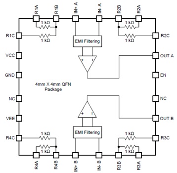
�D1.INA1620���ܿ�D
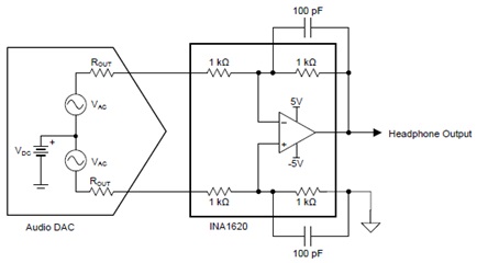
�D2.INA1620�����·:���C�Ŵ���
���C�Ŵ����OӋҪ��:
• ��5-V power supplies
• 150-mW output power (32-�� load)
• < �C110-dB THD+N at maximum output (32-�� load)
• < 0.01-dB magnitude deviation (20 Hz to 20 kHz)
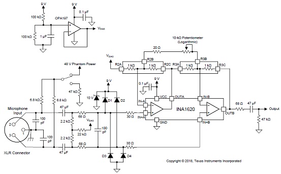
�D3.���I�����L�A�Ŵ����·
���l�Ŵ����u��ģ�KINA1620 EVM
This user��s guide contains information for the INA1620 device as well as support documentation for theINA1620 evaluation module (EVM). Included are the performance specifications, set-up procedure,modifications, measured data, printed circuit board (PCB) layout, schematic, and bill of materials (BOM) ofthe INA1620EVM.
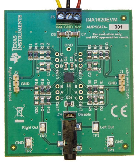
�D4.���l�Ŵ����u��ģ�KINA1620 EVM���ΈD
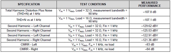
INA1620 EVM�yԇ���ܿ��Y:
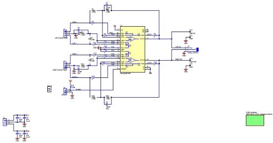
�D5.INA1620 EVM�·�D
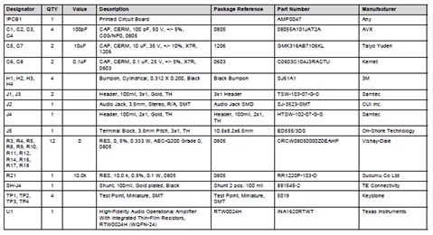
INA1620 EVM�������:
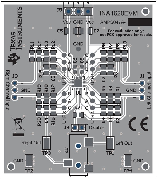
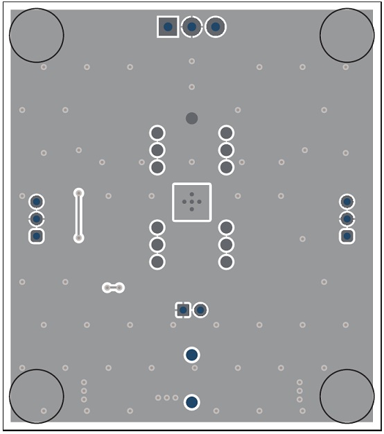
�D6.INA1620 EVM PCB�OӋ�D:플Ӳ���
�D7.INA1620 EVM PCB�OӋ�D:�Ӳ��� |
| |
|
|
|
|
|
| |
| |
| |
 |
�����܌����®aƷ���dȤ |
 |
|
 |
| �aƷ��̖ |
���ܽ�B |
������̖ |
���b��ʽ |
����늉� |
��ע |
| HT97180 |
2X125mW/4.2V/32�� |
SGM4917/MAX97220 |
QFN-16 |
1.65V-4.8V |
1.6V������늉����oPOP������ݲ��ݔ��125mW���wG��C�Ŵ�IC |
|
| |
|
| |
|
|